How to handle Piezotech products?
This section provides technical information about how to process Piezotech® P(VDF-TrFE) and P(VDF-TrFE-CTFE/CFE) products. You may find other information in our technical documents.
Also feel free to contact our technical team if you have any technical issue: Send a message
From ink formulation to poling
Piezotech® P(VDF-TrFE) and P(VDF-TrFE-CTFE/CFE) polymers are soluble in different solvents. Polymer concentration must be tuned in order to obtain the appropriate viscosity corresponding to your printing process. Polymer dissolution can be achived with very good mechanical stirring under moderate heating (below 80 °C). A filtration step is required to achieved high purity inks.
We also market inks that can be used directly (FC/RT inks).
| Boiling Point (°C) |
Flash Point (°C) |
|
|
Acetone |
56 |
- 18 |
|
Tetrahydrofuran |
65 |
- 17 |
|
Methyl Ethyl Ketone |
80 |
- 6 |
|
Methyl Isobutyl Ketone |
118 |
23 |
|
Glycol Ethers |
118 |
40 |
|
Glycol Ether Esters |
120 |
30 |
|
N-Butyl Acetate |
135 |
24 |
|
Dimethyl formamide |
153 |
67 |
|
Cyclohexanone |
157 |
54 |
|
Dimethyl acetamide |
166 |
70 |
|
Diaceton Alcool |
167 |
61 |
|
Diisobutyl Ketone |
169 |
49 |
|
Tetramethyl urea |
177 |
65 |
|
Ethyl Aceto Acetate |
180 |
84 |
|
Dimethyl Sulfoxide |
189 |
35 |
|
Trimethyl phosphate |
195 |
107 |
|
N-Methyl-2-Pyrrolidone |
202 |
95 |
|
Butyrolactone |
204 |
98 |
|
Isophorone |
215 |
96 |
|
Triethyl phosphate |
215 |
116 |
|
Carbitol Acetate |
217 |
110 |
|
Propylene Carbonate |
242 |
132 |
|
Glyceryl triacetate |
258 |
146 |
|
Dimethyl Phtalate |
258 |
149 |
Drying - Solvent Evaporation
In order to get rid of any residual solvent and enhance film properties, a solvent evaporation step under atmospheric pressure or under vacuum can be carried out below the solvent’s boiling-point temperature. Evaporation strongly depends on evaporation facilities and air flow. It can thus be performed from room temperature to 140 °C, depending on the product grade.
Annealing
Annealing is a critical step to obtain the films with the best properties. It will control crystallization of the material and enhance electrical as well as mechanical properties.
For P(VDF-TrFE) copolymers
Annealing should be performed between the Curie temperature and the melting point, in the paraelectric phase, for 2-15 min. This corresponds to a 135-145 °C range. For Piezotech® FC20, 80/20 P(VDF-TrFE), the 140-145 °C range is preferred.
%20Copolymers.png)
For P(VDF-TrFE) copolymers, annealing should be performed in the paraelectric phase, as close as possible to the melting.
For P(VDF-TrFE-CTFE/CFE) terpolymers
Films may need to be annealed at an appropriate temperature during a variable time from 3 to 20 min, typically 5-15 °C below the melting point. A rapid annealing may be obtained on thin films using Infrared or Flash annealing.
In order to activate their piezoelectric and ferroelectric properties, P(VDF-TrFE) copolymers layers must be poled to orientate the C-F dipoles. Contact poling with top and bottom electrode, or non-contact Corona poling with only the bottom electrode can be carried out.
Typical process for contact poling
AC or DC volage can be applied, at room temperature, up to twice the coercive field: 100 V.µm-1.
AC is advised with frequencies in the 0.1-10 Hz range.
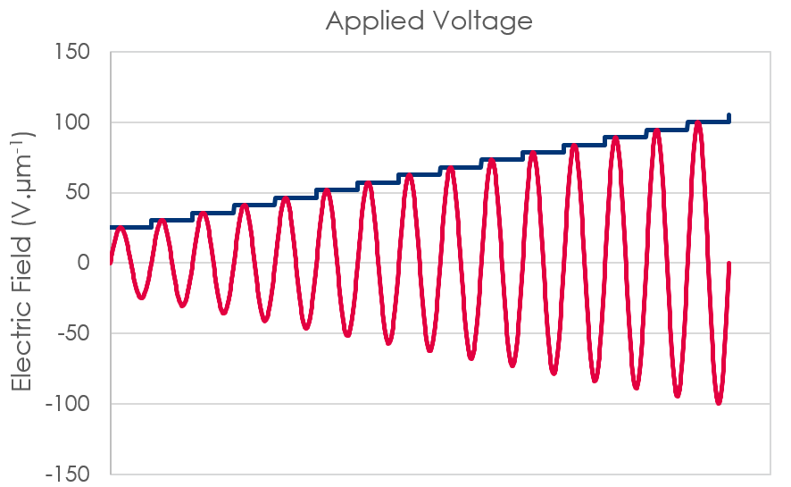
Example of DC (blue) and AC (red) voltage ramps to pole a P(VDF-TrFE) layer
Example
An electric field is applied according to the following cycle:
- Voltage ramp: 0 V.µm-1 to 100 V.µm-1
- Frequency: 1 Hz (higher is possible)
- Number of cycles to reach 100 V.µm-1: 15
- Signal wave form: Sinusoidal
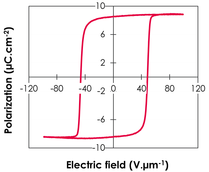
Typical ferroelectric loop of a P(VDF-TrFE) copolymer poled at 100 V.µm-1
Contact poling or Corona poling can be monitor by the current flowing through the P(VDF-TrFE) layer.
Case of contact poling
For contact poling with AC voltage, the current between top and bottom electrodes is proportional to the sum of the resistive current, capacitive current and polarization current. After substracting the capacitive and resistive components of the raw current, polarization current can be extracted and after integration give the ferroelectric loop.

Piezoelectric signal monitoring
Charge sensors
Concepts: A charge sensor generates on its surface equal electric charges of opposite sign when it is stimulated by a mechanical force (piezoelectric effect) or a variation of temperature (pyro electric effect).
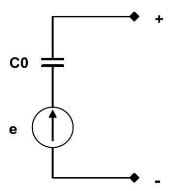
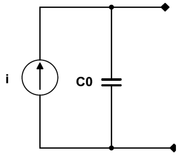
Equivalent diagrams: A piezo-, pyro- electric sensor can be modelled by one of the following equivalent diagrams:
|
Thevenin equivalent diagram: The electromotive force e = Q/C0 is in series with a capacitor C0.
|
Norton equivalent diagram: The current source i = dq/dt is in parallel with a capacitor C0.
|
Mode of operation: When using a piezo- pyro- electric sensor, the measured signal strongly depends on the conditions of experimentation. It is possible to measure a proportional signal, or to its derivate. The limit of these operation modes is given by the cut-off frequency of your instrumentation chain.
Signal conditioning
Direct connection: By connecting your sensor directly to your amplifier, oscilloscope, or DAC (data acquisition card) it must be kept in mind that external impedances may have a critical influence on the signal you will measure. In order to determine the said influences, the involved impedances (from the sensor, cable and measuring instrument input) are modelled as follows:
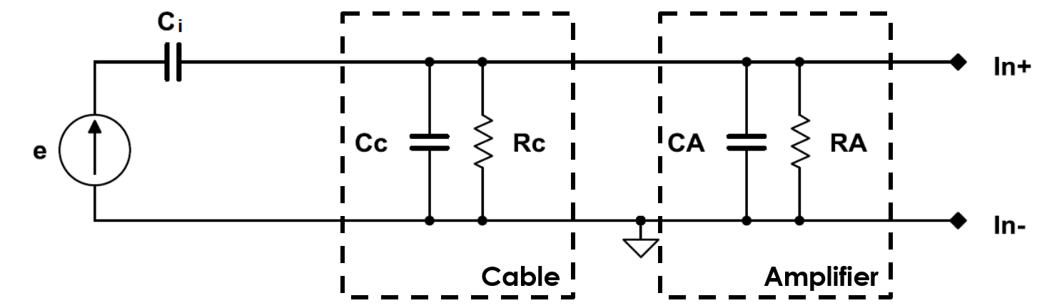
Equivalent diagram of a direct connection of a sensor
Further analysis of the diagram shows a high-pass filter behaviour, for which the cut-off frequency is given by:
 |
|
| When f >> fc, the measured signal is directly proportional to the generated charges: |
When f << fc, the measured signal is proportional to the derivate: |
 |
 |
Charge transducer
In order to drastically limit the influence of external impedances, the use of a charge transducer is recommended. The operating principle is based on the use of an external capacitor C to store the generated charges. A charge transducer may be also be called a charge-voltage converter.
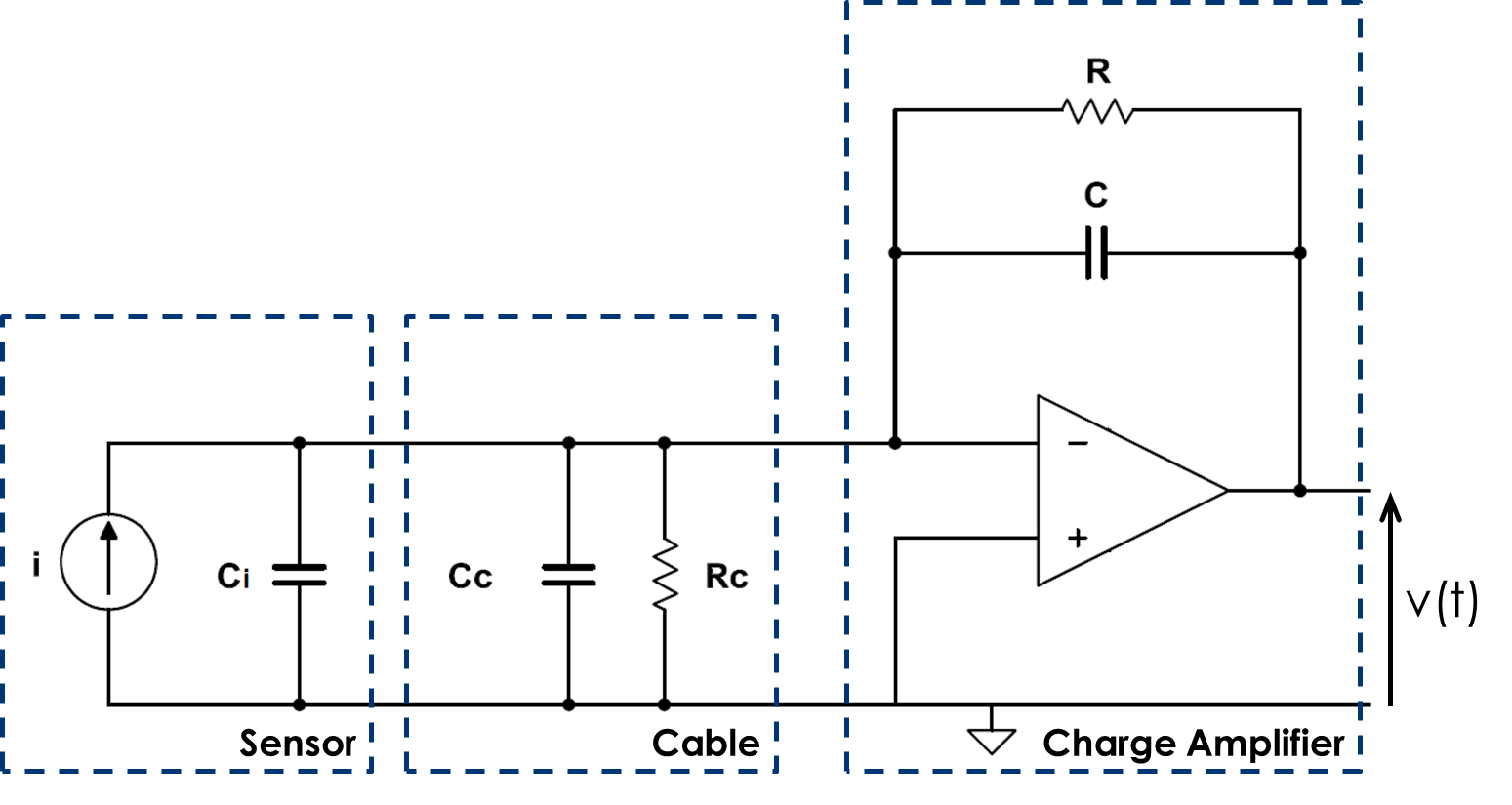
Practical implementation of a charge-voltage transducer
As shown in the diagram, we consider the operational amplificator as ideal. The differential voltage between its inputs is null, so the current i generated by the sensor is driven to the feedback capacitor C. In order to prevent saturation of the output by parasitic influences, a parallel resistor R must be added to the feedback capacitor.
Such a circuit has a high-pass filter behaviour, for which the cut-off frequency is given by:
 |
|
| When f >> fc, the measured signal is directly proportional to the generated charges: | When f << fc, the measured signal is proportional to the derivate: |
 |
 |
There are many options regarding the selection of a digital oscilloscope - a good range of "virtual" instruments (modules that simply plug in to ports on PC or laptop) is available from Digilent® (Analog Discovery 2, Discovery 2)
Deformation under electrical field
The deformation caused by the applied electric field can be defined by the simple formula:
Si = d3i.E
Where:
- Si = Δxi/xi = ΔL/L represents the strain (relative deformation) of the sample in the xi direction
- d3i is the piezoelectric strain constant (in a perpendicular direction with respect to that of the applied electric field)
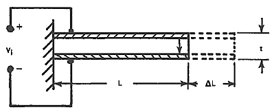
Example of an element with the following characteristics:
- Length: l = 1 cm
- Width: w = 2 mm
- Thickness: t = 9 µm
- Applied voltage: V = 200 V → E (electric field) = V/t
- (d31, d32, d33) = (11, 10, -30) pC.N-1
The piezo strain constant d is given by:
d = strain developped/applied field = S/E

Sensors: Orders of Magnitude, Voltage generation
The electric field output (E) caused by an applied force can be defined by:
E = gij.σi
Where:
- σi is the applied mechanical stress (N.m-2)
- gij is the piezoelectric voltage constant (Vm.Nm-2)
g = electrical field developed/applied mechanical stress = E/σ
with g = d/ε = d/εrε0

Example of an element with the following characteristics:
- Length: l = 2 cm
- Width: w =2 cm
- Thickness: t = 100 µm
- Compression 0.1 Bar → σ = -10000 N.m-2
- (g31, g32, g33) = (216, 19, -339) *10-3 - Vm.Nm-2
E = V0/t = g33.σ3
V0 = g33.σ3.t = 339 mV